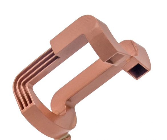
EMAG eldec is breaking new ground in the production of inductors for induction heating and relies on the latest manufacturing methods, such as additive manufacturing.
We discussed the advantages this provides and the new opportunities this opens up with Kadir Yilmazli, who is responsible for ongoing development in this area as a development engineer for additive manufacturing at EMAG eldec.
Mr. Yilmazli, you’re a development engineer for additive manufacturing at EMAG eldec, what exactly are your responsibilities?
In very broad terms, I’m responsible for introducing the process in the company and for adapting the development of inductors to the possibilities offered by additive manufacturing. In the past, inductors not only had to be designed around the component to be heated, but we also had to account for the limitations of the manufacturing process. Today, we no longer have these limitations and we enjoy much more freedom in the design process, which opens up new possibilities. I’m responsible for exploring these possibilities. To do this, I use numerical calculation to support optimal inductor design. I also optimize the actual additive manufacturing process.
Why did EMAG eldec choose to produce the components itself? Would it not have been easier and cheaper to subcontract coil manufacturing to a service provider once they have been designed?
For us here in Dornstetten, it is not only important to understand the entire process chain, but also to fully master it. There most likely is a historical reason for this. After all, it all began with inductor manufacturing. Today, EMAG eldec is a major manufacturer of generator technology, induction hardening machines and of course the corresponding inductors. We produce both the machines and the tools. This is where we simply need to master everything up and down the process chain. Ultimately, that’s the only way to become one of the best. However, aside from this philosophy, being involved in additive manufacturing technologies also provides a tremendous learning potential that ultimately leads to a potential for generating added value. You can only make full use of a technology if you know all of its ins and outs, and that’s why the experiences we gain in the manufacturing process directly end up in the design. In-house production also allows for fast response times and above all cost-optimized manufacturing.
Which additive manufacturing technology do you implement and why this one in particular?
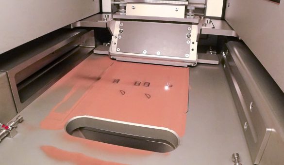
There are essentially two common processes for additively manufacturing inductors. These are Electron Beam Melting, EBM for short, and Selective Laser Melting, SLM for short. Because of its higher level of detail, the stability of the process and also the robustness of the method, we’re focusing on SLM. That is also the reason why the SLM method is gaining ground in inductor manufacturing. Nowadays, copper alloys are used with this method. While these have a somewhat lower electrical conductivity than pure copper, they are much stronger. According to present experience, inductors manufactured with SLM therefore have a much greater service life. Working pure copper currently is another major trend in the market. While it allows for maximum conductivity to be achieved, it leads to worse mechanical properties. Furthermore, pure copper requires a green laser, which is still very expensive. What the future holds in this respect is very thrilling. We are therefore closely monitoring these developments to obtain maximum quality from additive manufacturing for our inductors.


Could you describe what such a manufacturing process involves?
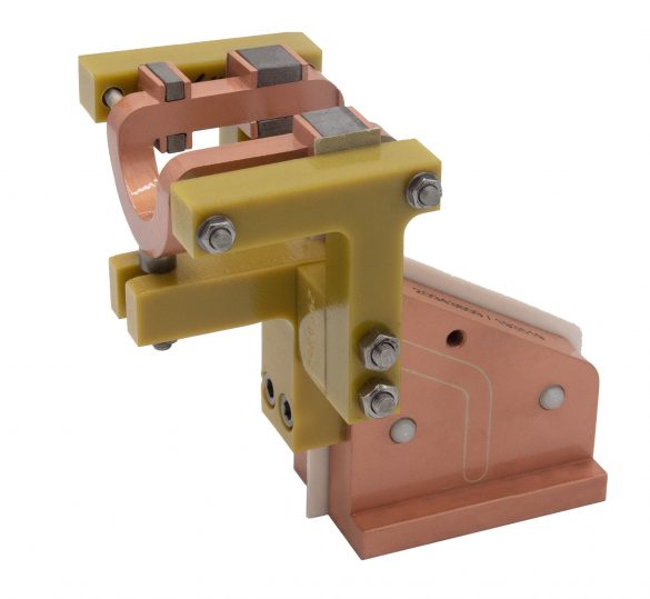
It essentially all begins with the design of the inductors, which are first matched to the desired heating result for the respective component. The coil’s cooling is then optimized, which involves performing digital flow calculation to achieve a perfect coolant flow. This is where we make full use of the freedom in design that we gain from using the method. It has significantly contributed to how we were able to considerably increase the service life of additively manufactured inductors. Once this part of the design has been completed, we proceed with adapting it to the manufacturing technology. For instance, this includes correct alignment of the component in the machine’s installation space and creating the support structures required to manufacture the coils with SLM. The actual manufacturing process begins after this step and takes about 8 to 16 hours depending on size. Once the parts have been completed, the support structures are removed, and the coils are heat treated. This not only provides an improved surface, but also maximizes the material’s electrical conductivity. The coil must then be soldered onto the inductor base. However, before the inductors leave our company, a quality control inspection is performed using a 3D measuring arm in order to ensure dimensional accuracy. Once they have passed inspection, they are delivered with the corresponding measurement report and a special case. That is how we are also able to ensure dimensional accuracy during transport.
That sounds like a very advanced method. Does this mean that in the future all inductors will be exclusively manufactured in this way?
No. Additive manufacturing enables us to be flexible and to produce a large part of our inductors economically and with high reproducibility. However, manual production remains more cost-effective when manufacturing particularly large inductors, for example for applications such as soldering shading rings. Additive manufacturing is not intended to serve as a sole replacement, but rather to extend our possibilities. It is mainly about exploring the limits of induction heating and doing so using special inductor geometries, which can either be particularly complex or particularly small. These are the outer limits into which we want to advance with the new manufacturing technology.
Mr. Yilmazli, thank you for this fascinating conversation.
